In-Depth Analysis Report on the Market Space and Investment Opportunities of Domestic Substitution for AFM Probes
Unlock More Features
Login to access AI-powered analysis, deep research reports and more advanced features
About us: Ginlix AI is the AI Investment Copilot powered by real data, bridging advanced AI with professional financial databases to provide verifiable, truth-based answers. Please use the chat box below to ask any financial question.
Based on the collected market data and research materials, I will prepare a detailed analysis report for you.
Atomic Force Microscope (AFM) probes are core components of atomic force microscopes, consisting of micron-scale cantilevers and nano-scale tips. Their performance directly determines detection accuracy [1]. AFM probes play an irreplaceable role in semiconductor inspection, mainly applied in:
- Advanced Process Inspection: As chip process nodes evolve to 5nm and below, the precision requirements for nano-scale defect inspection continue to increase
- Material Surface Topography Analysis: Provides atomic-level 3D surface topography images with atomic-level resolution [2]
- Semiconductor Process Control: Used for measuring parameters such as wafer surface roughness, particle size, and pore size distribution
According to Intel Market Research data, the global AFM probe market shows steady growth:
| Year | Market Size (Million USD) | YoY Growth Rate |
|---|---|---|
| 2024 | 236 | Base Year |
| 2025 | 255 | 8.1% |
| 2026 | 276 | 8.2% |
| 2027 | 298 | 8.0% |
| 2028 | 322 | 8.1% |
| 2029 | 348 | 8.1% |
| 2030 | 376 | 8.0% |
| 2031 | 406 | 8.0% |
| 2032 | 403 | -0.7% |
The Chinese semiconductor inspection equipment market scale continues to expand:
| Year | Market Size (Million USD) | YoY Growth Rate |
|---|---|---|
| 2019 | 1310 | - |
| 2020 | 1870 | 42.7% |
| 2021 | 2960 | 58.3% |
| 2022 | 2830 | -4.4% |
| 2023 | 3670 | 29.7% |
| 2024E | 3750 | 2.2% |
| 2025E | 4130 | 10.1% |
The global AFM probe market presents a highly concentrated competitive landscape:
| Ranking | Enterprise | Market Share | Features |
|---|---|---|---|
| 1 | NanoWorld AG | ~35% | World’s largest supplier |
| 2 | Bruker Corporation | ~35% | Technology leader, dominates high-end market |
| 3 | NT-MDT Spectrum Instruments | ~10% | Focuses on mid-end market |
| 4 | Asylum Research (Oxford Instruments) | ~8% | High-end scientific research-grade products |
| 5 | Olympus Corporation | ~5% | Dominates Japanese market |
| 6 | Others | ~7% | Regional suppliers |
The global semiconductor metrology and inspection equipment market is also highly concentrated:
| Enterprise | Global Market Share | Core Advantages |
|---|---|---|
| KLA | 55.8% | Comprehensive technology, monopoly in high-end market |
| Applied Materials (AMAT) | 10%+ | Integrated solutions |
| Hitachi High-Technologies | 8%+ | Leading in CD-SEM segment |
| ASML | 6%+ | Electron beam inspection |
The localization rate of Chinese semiconductor equipment is increasing rapidly:
| Equipment Category | 2020 | 2021 | 2022 | 2023 | 2024E | 2025E |
|---|---|---|---|---|---|---|
| Overall Semiconductor Equipment | 2% | 5% | 21% | 35% | 42% | 50% |
| Metrology/Inspection Equipment | <1% | <2% | <3% | <5% | <8% | <10% |
| Lithography Equipment | <1% | <1% | <1% | <1% | <1% | <1% |
| Etching Equipment | 5% | 8% | 12% | 15% | 20% | 25% |
| Thin Film Deposition Equipment | 5% | 8% | 12% | 18% | 25% | 30% |
The market space calculation is based on the following assumptions:
- Global AFM Probe Market: $236 million in 2024, CAGR 8.1%
- Chinese Market Share: Assume China accounts for 25-30% of the global market
- Current Localization Rate: Less than 1% (almost completely dependent on imports)
- Target Localization Rate: Reach 30% within 5 years
| Indicator | 2024 | 2025 | 2027 | 2030 |
|---|---|---|---|---|
| Chinese AFM Probe Market Size (Million RMB) | 420 | 450 | 530 | 680 |
| Domestic Substitution Space (Million RMB) | 416 | 441 | 477 | 476 |
| Target Localization Rate | 1% | 5% | 15% | 30% |
| Accessible Market for Domestic Manufacturers (Million RMB) | 4 | 23 | 80 | 204 |
| Equipment Type | Global Market (Million USD) | Chinese Market (Million USD) | Localization Rate | Domestic Substitution Space (Million USD) |
|---|---|---|---|---|
| Optical Inspection Equipment | 8900 | 3100 | 3% | 3010 |
| Electron Beam Inspection Equipment | 2500 | 860 | <1% | 850 |
| CD-SEM Equipment | 1800 | 620 | <5% | 590 |
| AFM and Related Probes | 236 | 82 | <1% | 81 |
Total |
13436 |
4662 |
<5% |
4531 |
| Item | Information |
|---|---|
| Company Name | Tanzhen Nano Technology Co., Ltd. |
| Founder | Professor Cui Bo (Peking University) |
| Financing Status | Over RMB 10 million in Pre-A/A Round |
| Core Technology | Dry Etching Process |
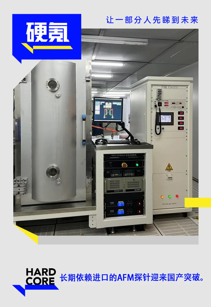
| Core Breakthrough | The only domestic enterprise manufacturing probes from wafers |
Tanzhen Nano has achieved mass production of probes from wafers using the
| Technical Route | Traditional Wet Etching | Dry Etching (Tanzhen Nano) |
|---|---|---|
| Precision Control | Micron-level | Nano-level |
| Process Consistency | Low | High |
| Mass Production Capacity | Limited | Scalable mass production |
| Cost | Medium | Relatively low |
| Environmental Pollution | Significant | Minor |
Tanzhen Nano’s subsidiary, Tanwei Nano, has overcome the challenge of
- Ultra-High Alignment Precision: Significantly improves the consistency of chip mounting positions, solving the problem of precise alignment at the micro-nano scale
- Process Stability: Greatly reduces uncertainties caused by manual operations, ensuring high product yield
- Production Efficiency Improvement: Realizes automated production, reducing production costs
| Indicator | International Brands | Tanzhen Nano | Advantages |
|---|---|---|---|
| Price | Benchmark | 30-40% lower | Significant cost advantage |
| Partial Performance Indicators | Benchmark | Partial leading indicators | Technological breakthrough |
| Delivery Lead Time | 4-8 weeks | Shorter | Localization advantage |
| Technical Support | Limited | Timely response | Local service advantage |
| Advantage Dimension | Specific Performance | Score (Full 100) |
|---|---|---|
| Technological Innovation | Dry etching + high-precision chip mounting process | 85 |
| Cost Advantage | 30-40% lower price | 90 |
| Domestic Substitution Space | 99% import dependence | 95 |
| Capital Attention | Completed over RMB 10 million in financing | 80 |
| Market Timing | Domestic substitution window period | 88 |
According to SEMI data, the value distribution of wafer manufacturing equipment is as follows:
| Equipment Category | Value Share | Localization Rate | Investment Priority |
|---|---|---|---|
| Lithography Equipment | 30% | <1% | ★★★★★ |
| Etching Equipment | 22% | 15-20% | ★★★★☆ |
| Thin Film Deposition | 18% | 15-20% | ★★★★☆ |
| Metrology/Inspection Equipment | 11% | <5% | ★★★★★ |
| Cleaning Equipment | 6% | 20-30% | ★★★☆☆ |
| CMP Equipment | 5% | 20-30% | ★★★☆☆ |
| Others | 8% | - | ★★☆☆☆ |
Semiconductor Inspection Equipment Industrial Chain
├── Upstream
│   ├── AFM Probes/Consumables (market size: $236 million) ◄ Tanzhen Nano's segment
│   ├── Electron Beam Sources
│   ├── Optical Components
│   └── Precision Mechanical Components
├── Midstream
│   ├── Optical Inspection Equipment (market size: $8.9 billion)
│   ├── Electron Beam Inspection Equipment (market size: $2.5 billion)
│   ├── CD-SEM Equipment (market size: $1.8 billion)
│   └── AFM Equipment (small market size but critical)
└── Downstream
    ├── Wafer Fabrication Plants (Semiconductor Manufacturing International Corporation (SMIC), Yangtze Memory Technologies Co., Ltd. (YMTC), ChangXin Memory Technologies, Inc. (CXMT), etc.)
    ├── Packaging and Testing Plants
    └── Research Institutions
| Dimension | Evaluation | Score |
|---|---|---|
| Market Size | Global $236 million, Chinese market ~RMB 420 million | ★★★☆☆ |
| Growth Potential | CAGR 8.1%, accelerated domestic substitution | ★★★★☆ |
| Competition Intensity | Dominated by international giants, early stage of domestic substitution | ★★★★☆ |
| Technological Barriers | High (Tanzhen Nano has achieved breakthroughs) | ★★★★★ |
| Policy Support | Core segment for semiconductor self-sufficiency | ★★★★★ |
Comprehensive |
Domestic substitution window period |
★★★★☆ |
- Market Rigid Demand: AFM probes are consumable core components for semiconductor inspection, with sustained demand
- Domestic Blank: 99% reliance on imports, a breakthrough opportunity from 0 to 1 for domestic substitution
- Technological Leadership: Tanzhen Nano has achieved mass production from wafers, with unique domestic technology
- Cost Advantage: 30-40% lower price, with cost-performance competitiveness
- Policy Dividends: Semiconductor self-sufficiency has become a national strategy, with continuous policy support
- Increase in the localization rate target of semiconductor equipment (50% by 2025)
- Establishment of the third phase of the National Integrated Circuit Industry Investment Fund (registered capital of RMB 344 billion)
- Accelerated expansion of Yangtze Memory Technologies Co., Ltd. (YMTC) and ChangXin Memory Technologies, Inc. (CXMT)
- Growing anxiety over overseas supply chain security
| Risk Type | Specific Content | Impact Level |
|---|---|---|
| Technical Risk | Product stability and consistency require time for verification | Medium |
| Market Risk | Strong customer loyalty to international brands, challenges in brand building | High |
| Competition Risk | Possible price wars with international brands | Medium |
| Capital Risk | Continuous R&D requires substantial capital investment | Medium |
| Policy Risk | Cyclical fluctuations in the semiconductor industry | Low |
Tanzhen Nano’s technological breakthrough fills the
- From None to Existence: The first domestic mass production of AFM probes from wafers
- From Following to Parity: Some performance indicators reach international leading levels
- From Import to Domestic Production: Reducing dependence on international brands
Tanzhen Nano's Technological Breakthrough
│
├── Upstream Synergy
│   ├── Semiconductor Materials (silicon wafers, photoresists, etc.)
│   ├── MEMS Processing Equipment
│   └── Precision Measuring Instruments
│
├── Horizontal Synergy
│   ├── China Test Microelectronics Co., Ltd. (Metrology and Inspection Equipment)
│   ├── Wuhan Jingce Electronics Co., Ltd. (Inspection Equipment)
│   └── Shanghai Ralee Technology Co., Ltd. (Metrology Equipment)
│
└── Downstream Synergy
    ├── Wafer Fabrication Plants
    ├── Research Institutes
    └── Semiconductor Material Enterprises
Under the current international situation, semiconductor supply chain security has become a core concern:
- Reduced Supply Disruption Risk: AFM probes are no longer completely dependent on imports
- Improved Bargaining Power: Forming a competitive landscape, breaking price monopolies
- Accelerated Technological Iteration: Faster response of localized services and more timely technical support
Tanzhen Nano’s technological breakthrough promotes the improvement of the
| Ecosystem Element | Current Status | Future Trend |
|---|---|---|
| Core Components | Dependent on imports | Partially localized |
| Complete Equipment | 少量 localized | Accelerated substitution |
| Materials and Consumables | Low-end localized | Comprehensive breakthroughs |
| Process Technology | Following and learning | Independent innovation |
| Talent Reserve | Shortage | University-industry-institute cultivation |
Tanzhen Nano’s successful case has a
- Technological Path Verification: Proving that domestic enterprises can achieve breakthroughs in high-end precision manufacturing
- Commercialization Path Verification: The path from laboratory to mass production is feasible
- Capital Exit Path Verification: The investment logic of hard technology is verified
Tanzhen Nano’s technological breakthrough will support the
| Application Field | Application Scenario | Demand Growth |
|---|---|---|
| Semiconductor Manufacturing | Nano-scale defect inspection | 15-20%/year |
| Materials Science | Surface topography analysis | 10-15%/year |
| Life Sciences | Biological sample imaging | 12-18%/year |
| Nanotechnology | Nanodevice manufacturing | 20-25%/year |
| Quantum Technology | Quantum material characterization | 25-30%/year |
| Dimension | Evaluation | Conclusion |
|---|---|---|
Market Space |
Global $236 million, Chinese market ~RMB 420 million | Medium scale, high growth |
Domestic Substitution |
99% import dependence, localization rate <1% | Huge substitution space |
Technological Breakthrough |
Dry etching + high-precision chip mounting | Domestic leading, on par with international levels |
Competitive Advantage |
30-40% cost advantage | Significant cost-performance |
Investment Timing |
Domestic substitution window period | Best entry timing |
Comprehensive Rating |
★★★★☆ | Recommended Attention |
- Policy Window: The third phase of the National Integrated Circuit Industry Investment Fund has been established, with unprecedented policy support
- Market Window: Semiconductor cycle recovery, accelerated domestic substitution
- Technological Window: Tanzhen Nano has completed technological breakthroughs and entered the industrialization stage
- Capital Window: Hard technology investment has become a hot spot, with a friendly financing environment
| Strategy Type | Specific Recommendations |
|---|---|
| Early-stage Investment | Focus on Tanzhen Nano |
Insights are generated using AI models and historical data for informational purposes only. They do not constitute investment advice or recommendations. Past performance is not indicative of future results.
About us: Ginlix AI is the AI Investment Copilot powered by real data, bridging advanced AI with professional financial databases to provide verifiable, truth-based answers. Please use the chat box below to ask any financial question.